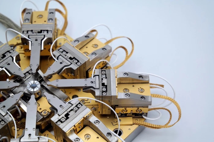
The SMARPROBE Nanoprober from SmarAct Metrology GmbH und Co. KG, sets new standards for failure analysis of semiconductor chips and electrical characterization of nanomaterials. The novel closed-loop motion system enables automated and reliable contacting and manipulation in PROBE Etch to produce tungsten tips with the smallest tip radius of 8 nm, to the integration of the SMARPROBE Prober, which can be installed directly into an existing microscope at the customer's site.
The SMARPROBE motion system consists of up to eight manipulators, ithe nanometer range.
The continuing miniaturization trend of a wide variety of technologies as well as the development of new materials with increasingly complex structures makes localization of defects increasingly difficult. Such high-end applications within electron microscopes, as well as simpler light microscope applications, require reliable high-precision equipment for defect analysis and electrical characterization. With its Nanoprober, SmarAct Metrology offers complete solutions specifically designed for this purpose – starting with the SMARncluding a measuring tip holder and a sample stage, each based on the latest SmarAct positioning technology. The motion system is closed-loop controlled, allowing very precise and stable positioning with 1 nm resolution. The sample area of 30 x 30 mm provides sufficient space to directly place multiple samples. The active temperature control of the system makes it possible to achieve stable electrical contacting of multiple probe tips on a probe, such as single transistors of 5-nanometer technology, even under non-stable thermal environmental conditions.
The measuring needles and the sample can be navigated automatically via absolute values (CAD) or intuitively via "point-and-click" in the microscope image. To simplify the landing of the probes on the sample, the "Advanced Probe Holder" allows automatic contacting on any material, regardless of conductivity. This allows automation of customer-specific movement and measurement sequences, using Python scripting within the SmarProbe software. The software includes the control of a parameter analyzer. In addition, each probe has an integrated low-noise current amplifier for fast and low-noise measurement of currents, which can be used e.g., for imaging of electron beam absorption (EBAC).


