
 Login/Register
 Supplier Login


At the 2025 SEMICON exhibition, HIWIN is showcasing their precision key components and mechatronic integration capabilities, delivering high-precision smart manufacturing solutions tailored for the semiconductor industry. Guided by the philosophy of being the “Best Partner in Smart Manufacturing,” HIWIN has become the preferred partner of the world’s top three semiconductor equipment manufacturers. This achievement is driven by HIWIN’s comprehensive solutions and differentiated, real-time global service.
HIWIN has also received accolades such as Best Supplier Award and Best Quality from Applied Materials (AMAT), a leading global semiconductor equipment manufacturer. This recognition highlights HIWIN’s consistent excellence in quality, reliability, and service within the highly demanding semiconductor industry.
Visitors are invited to the SEMICON Southeast Asia 2025 from May 20–22, 2025, at the Sands Expo and Convention Centre, Singapore, Booth L2109, and discover HIWIN’s next-generation smart solutions for semiconductor processing.
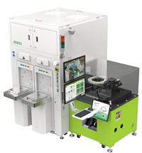 EFEM + DMT (Direct Drive Motor)
High-Precision Wafer AOI Inspection and EFEM Production Solutions - To meet the evolving demands of advanced packaging such as COWOS and FOPLP, HIWIN introduces high-precision large and medium hollow positioning platforms.
High-Precision Wafer AOI Inspection and EFEM Production Solutions - To meet the evolving demands of advanced packaging such as COWOS and FOPLP, HIWIN introduces high-precision large and medium hollow positioning platforms. These platforms, often requiring highly flexible delivery schedules, are supported by a complete granite material logistics supply chain. Additionally, HIWIN’s vertical integration of hardware and software creates a comprehensive automated wafer handling system (EFEM), providing effective semiconductor production solutions.
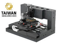 Nano Positioning Stage N2
High-End Inspection Equipment Solutions – Nano Positioning Stage N2 addresses the complexities of semiconductor processes and continually evolving inspection and measurement needs with high precision and stability. High-End Inspection Equipment Solutions – Nano Positioning Stage N2 addresses the complexities of semiconductor processes and continually evolving inspection and measurement needs with high precision and stability. N2 integrates mechanical, electrical, and software components to achieve nano-level positioning, reducing development time for high-end inspection equipment and enhancing market competitiveness.