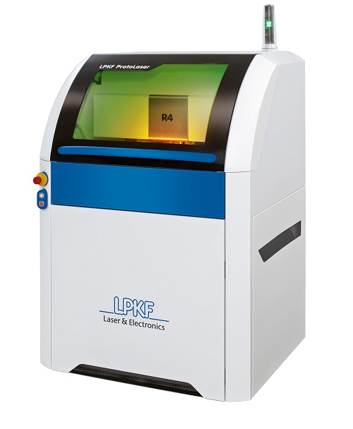
 Gallium nitride (GaN) substrates can be used in power interconnects and radio-frequency electronics for wireless communications. In the development of power electronics, they are increasingly being considered as substitutes for silicon-based chips and circuits. Application areas include 5G, defense and commercial aerospace, and satellite communications. However, processing of metal-plated gallium nitride-based ceramic materials can be challenging if the materials are composed of thin conductive metal layers on thick brittle ceramic substrates and both must be processed by machine. With the LPKF ProtoLaser R4, prototyping and production of low-volume quantities within the scope of research and development activities are easily done.
To process both material layers rapidly and cleanly – despite their greatly divergent material properties and required final specifications – the processing system must be accurate, adaptable, and tunable. The LPKF ProtoLaser R4 was developed for laser processing of new and unique materials in research settings. The ability to structure delicate substrates with high precision and cut hardened or fired engineered substrates afforded by its picosecond laser makes it the perfect tool for GaN. With virtually no heat input into the surrounding material, the system cuts and ablates the desired materials in a "cold," gentle, and precise process.
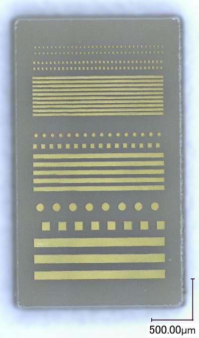
 With this laser-based process, two traditionally separate manufacturing steps – dicing of the ceramic substrate and etching of the conductive layer – can be done in a single contactless and chemical-free operation. This was demonstrated in feasibility studies performed at the University of Ljubljana (Slovenia). The ProtoLaser R4 first cut the ceramic material without introducing cracks or stresses and then micro-etched the top layer, which was gold in this case, without requiring any further user intervention. The laser power and pulse energy were adapted accordingly for the specific application.
This is just one of many possible, albeit special, applications for the LPKF ProtoLaser R4, which is equally well suited to cutting, drilling, and structuring typical materials for RF electronics, PTFE, double-sided flexible PCB laminates, thin metal layers on glass, etc., with high precision.
More information: www.lpkf.com/protolaser-r4

 Login/Register
 Supplier Login


