
 Login/Register
 Supplier Login


Panasonic Corporation announced that it has developed a sheet-form encapsulation material (CV2008 series) for coreless package substrates that enables thinner-profile and lower-cost semiconductor packages. The sheet-form encapsulation material, scheduled for mass production starting this month, is optimized for the insulation layers of coreless package substrates. Its suitability for large-area encapsulation allows thinner packages to be manufactured at lower cost.
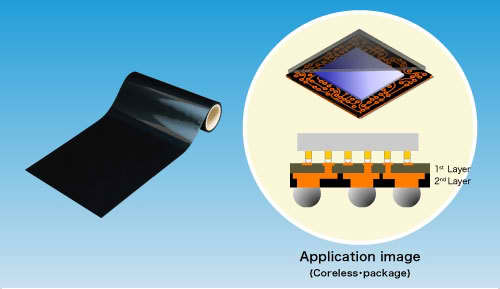
This new product has a uniformly produced insulation layer thickness that is ideal for the new coreless process, as it eliminates the need for laser drilling processing. The insulation layer for a package substrate can be produced using a large-area press process, enabling the mass production of packages at lower cost. The sheet thickness available comes in the range of 20 - 200 µm. The high rigidity of the thin sheet encapsulation material minimizes any warpage of packages and contributes to a thinner profile. Modulus of elasticity: 17000 MPa at 25°C. A low shrinkage rate of material, 0.003%, ensures connection reliability to be maintained during high-temperature reflow processes, increasing the production yield of the package assembly process.
Panasonic Corporation has been engaged in the development of diverse electronics technologies and solutions for customers in the consumer electronics, housing, automotive, enterprise solutions and device industries.